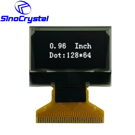
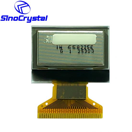
SCE096003-V01是一个COG型的OLED显示器,128×64分辨率,SSD1306BZ IC,4线串行接口,30针
型号:
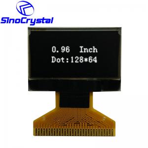
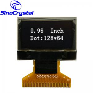
SCE096003-V01Size (inch)尺寸(英寸):
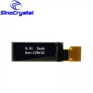
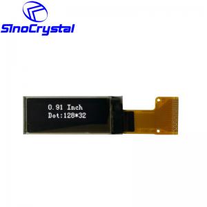
0.96寸Resolution:
128×64Outline Dimension (mm):
26.70×19.26×1.41Viewing Area (mm):
23.74x12.864Active Area (mm):
21.744×10.864Interface:
6800/8080 Interface/I2C/ 4-wire SPIIC Part No.:
SSD1306BZColor:
Monochrome (White)PIN:
30FPC type:
Soldering
Basic Information
Display Color: Blue
Dot Matrix: 128×64
Drive IC: SSD1306BZ
Viewing Angle: 160°
Aperture rate: 78%
Interface: 6800/8080 interface, 4 wire serial interface, I2C
Outline Dimension: 26.7(W)x19.26(H)x1.227(D)
View area: 23.74 (W) x 13.2(H)
PIN: 30
FPC Type: Soldering
Drawing

General Specification
| ITEM | SPECIFICATIONS | UNIT |
| MODULE SIZE | 26.7(W)x19.26(H)x1.227(D) | mm |
| VIEWING AREA | 23.74 (W) x 13.2(H) | mm |
| ACTIVE AREA | 21.74(W) x11.2 (H) | mm |
| DOT SIZE | 0.15(W) x0.15(H) | mm |
| DOT PITCH | 0.17(W) x0.17 (H) | mm |
| ASSY.TYPE | COG | --- |
| WEIGHT | TBD |
|
Interface Definition
| PIN NO. | SYMBOL | TYPE | FUNCTION DESCRIPTIONS |
| 1 | NC(GND) | P | It should be connected to external ground. |
| 2 | C2P |
|
C1P/C1N-Pin for charge pump capacitor. C2P/C2N-Pin for charge pump capacitor. Connect to each other with a capacitor. They must be floated when the Charge pump not use. |
| 3 | C2N |
|
|
| 4 | C1P | I | |
| 5 | C1N |
|
|
| 6 | VBAT | P |
Power supply for charge pump regulator circuit. It must be connected to external source when charge pump is used. It must be float when charge pump is not used. |
| 7 | NC |
|
NC |
| 8 | VSS | P | Ground pin. It must be connected to external ground. |
| 9 | VDD | P | Power pin for logic circuit. It must be connected to external source. |
| 10 | BS0 | I |
Interface selection pins.
|
| 11 | BS1 | ||
| 12 | BS2 | ||
| 13 | CS# | I | Chip Select input pin. Active "L" |
| 14 | RES# | I | Hardware reset input pin. Active "L". |
| 15 | D/C# | I |
This is Data/Command control pin. When the pin is pulled HIGH, the data at D[7:0] is data. When the pin is pulled LOW, the data at D[7:0] is command. In I2C mode, this pin acts as SA0 for slave address section. When 3-wire serial interface is selected, this pin must be connected to VSS |
| 16 | R/W# | I |
This is read/write control input pin. 8080: data write enable; 6800: read/write select pin. When serial or I2C interface is selected, this pin must be connected to VSS. |
| 17 | E# | I |
This is read/write control input pin. 8080: data read enable; 6800: read/write enable pin. When serial or I2C interface is selected, this pin must be connected to VSS. |
| 18 | D0 | I/O |
These are 8-bit bi-directional data bus to be connected to microprocessor's Data bus. When serial interface mode is selected, D2 should be kept NC, D1 will be the serial data input: SDIN, D0 will be the serial clock input: SCLK. When I2C mode is selected, D2, D1 should be tied together and serve as SDA and D0 is the serial clock input, SCL. |
| 19 | D1 | ||
| 20 | D2 | ||
| 21 | D3 | ||
| 22 | D4 | ||
| 23 | D5 | ||
| 24 | D6 | ||
| 25 | D7 | ||
| 26 | IREF |
I |
Current reference for brightness adjustment. This is segment output current reference pin. A resistor should be connected between this pin and VSS .Set the current at 12.5 uA maximum. |
| 27 | VCOMH | O |
COM signal deselected voltage level. A capacitor should be connected between this pin and VSS. |
| 28 | VCC |
P |
Power supply for OLED driving voltage. A capacitor should be connected between this pin and VSS, when charge pump is used. It must be connected to external source when charge pump is not used. |
| 29 | VLSS | P | This is an analog ground pin. It should be connected to VSS externally. |
| 30 | NC(GND) | P | It should be connected to external ground. |